Networking Communications
SEMANA 11: NETWORKING AND COMMUNICATIONS
Networking and Communications
Redes y Comunicaciones
This week the design and implementation of communication networks between electronic devices was explored, allowing different boards to exchange information through communication protocols.
Networks in embedded systems allow multiple microcontrollers to work in a coordinated manner, sharing data from sensors or sending signals to actuators. This type of communication is essential in applications such as automation, Internet of Things (IoT), smart agriculture and distributed industrial systems.
The objective of this activity was to design and implement a communication system between electronic boards, using communication protocols and ensuring that each node has an address or identity within the network.
Group Assignment
Sending messages between two projects
In the group task we worked on the implementation of communication between two electronic devices, allowing one system to send information and another system to receive it.
The objective was to understand how devices can exchange data through a communication protocol, verifying that the message sent by a node is correctly interpreted by the receiving node.
For this test we used:
A board with ATmega328P
A second plate to receive the information
Comunicación mediante protocolo serial
The system works as follows:
Un dispositivo genera un mensaje o señal.
This message is sent through the communication protocol.
The second device receives the message.
The receiving node interprets the information and performs an action, such as activating an LED or displaying information on a screen.
This exercise allowed us to understand the basic principles of data transmission, synchronization and verification of signals in a network of electronic devices.
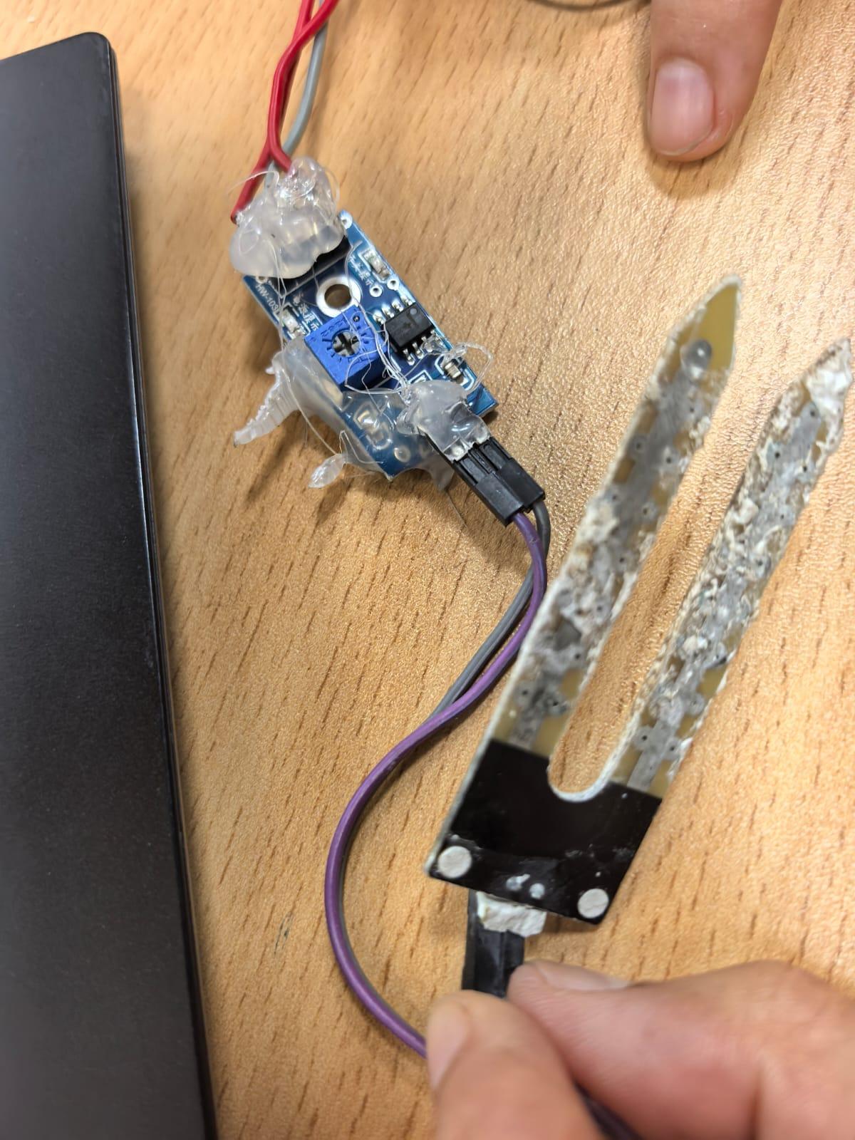
Photo of the complete assembly of the group working or the two connected plates
Text below photo:
Figure 1. Experimental setup used to test communication between devices.
Individual Assignment
Design of communication nodes
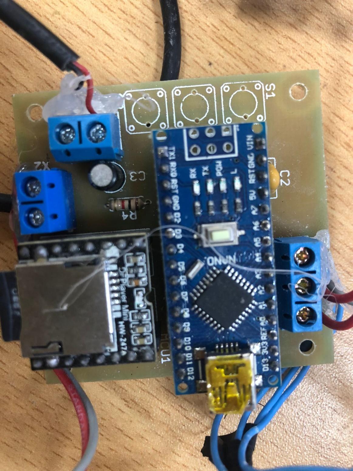
For the individual task I designed a system where two electronic nodes can communicate with each other, using an ATmega328P based board that was previously designed and manufactured in a previous assignment.
The system was developed to integrate:
An HL-69 soil moisture sensor as an input device
An LCD screen and an LED as output devices
Communication between devices using network protocol
Each board within the system has an identity within the network, which allows the nodes that participate in the communication to be differentiated.
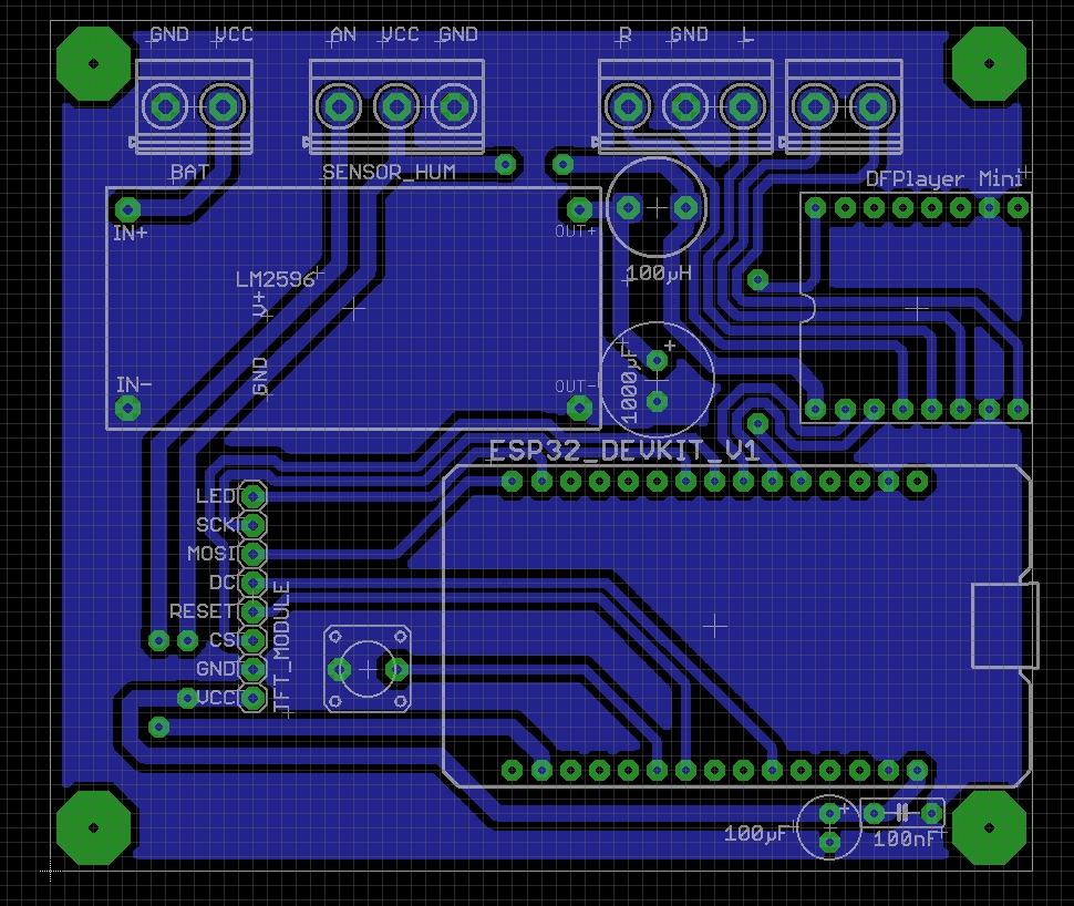
Photo of your PCB designed by you
Texto debajo:
Figure 2. ATmega328P based board used as a node within the communication system.
Network Workflow
Workflow in network design
The development of the network followed the following workflow:
Electronic system design
A board based on ATmega328P, designed previously in the course, was used.
Sensor integration
The HL-69 soil moisture sensor was connected to generate information about the environment.
Communication protocol implementation
The microcontroller was programmed to send and receive data using serial communication.
Data interpretation
The system processes the received signal and activates an LED or displays a message on the LCD screen.
This flow allowed us to understand how devices can be integrated into a distributed communication network.
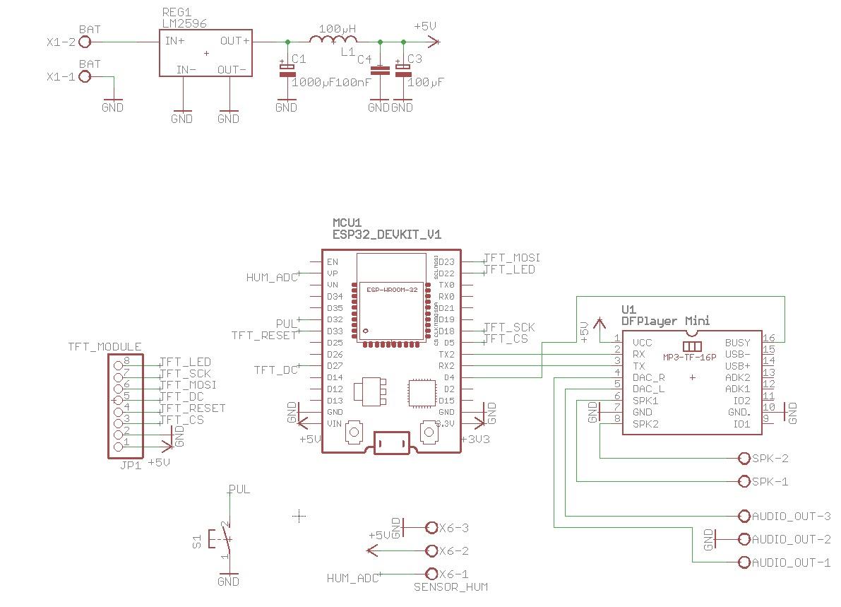
Photo of the complete connected circuit
Figure 3. Connection of the humidity sensor, LCD display and microcontroller in the system node.
Network Addressing
Network addressing
To ensure that each device within the network can be correctly identified, node addressing was used.
Each board is configured with a unique identity within the system, allowing messages to be sent to the correct node.
This approach is essential in microcontroller networks, as it avoids communication conflicts and allows multiple devices to share the same transmission channel.
📷 Photo of connection diagram or network scheme
Figure 4. Scheme of the communication system between nodes.
Programming Process
Programming process
The system programming was carried out using the Arduino IDE environment, adapting the code for the ATmega328P microcontroller.
The program is responsible for:
Read the humidity sensor signal
Interpret the state of the soil
Send or receive messages on the network
Activar indicadores visuales
The code was developed from base examples, but was modified to adapt it to the specific functionality of the project, integrating the sensor, the LED and the LCD screen.
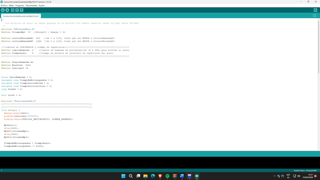
Screenshot of the code in Arduino IDE
Figure. Code developed to manage communication between nodes and sensor reading.
Problems and Solutions
Problemas encontrados y soluciones
Some technical challenges arose during the development of the project.
Device recognition
Initially, there were problems in communication between the devices due to incorrect configurations on the transmission pins.
Solution: Revised pin configuration and adjusted system addressing.
Communication with LCD screen
There were difficulties when integrating the LCD screen using the I2C protocol.
Solution: The code was modified to ensure correct initialization of the LCD module and its I2C address.
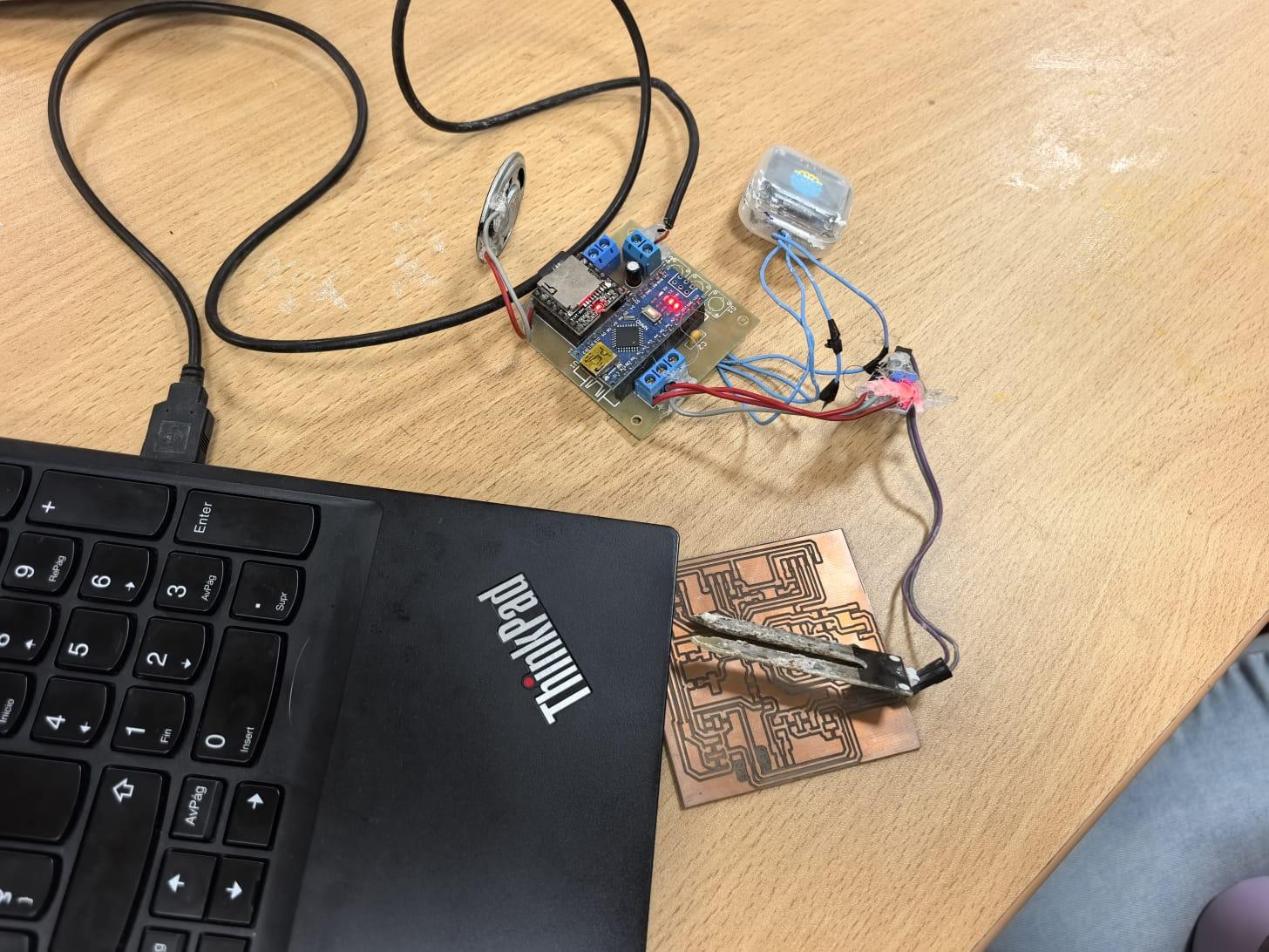
Photo of the system working
Figure. System in operation showing sensor status.
What I Learned
Reflexión personal
This activity provided a practical understanding of how microcontrollers can communicate with each other within an electronic network.
I learned the importance of:
Implement communication protocols
Manage network addresses
Integrate sensors within distributed systems
Resolve communication problems between devices
Furthermore, this experience demonstrates how it is possible to develop intelligent electronic systems capable of exchanging information, which is the basis of modern technologies such as the Internet of Things (IoT).