Embedded Programming
Semana 08: Electronics Production
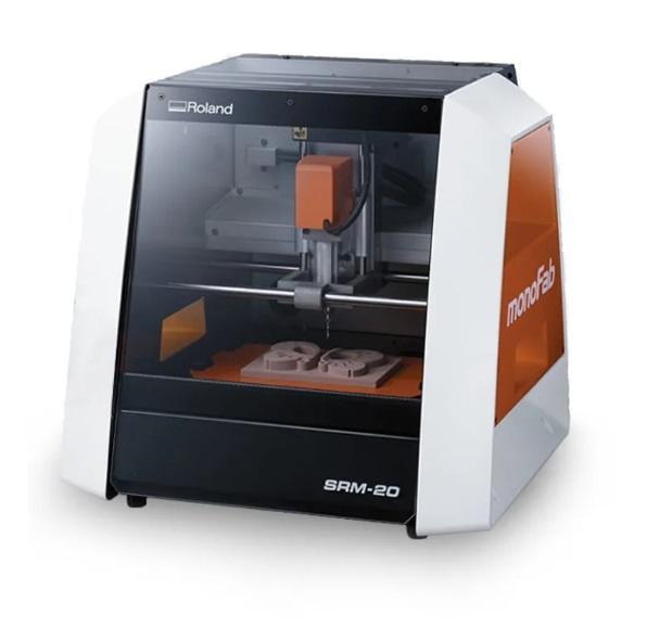
For the group task, use the operation of the Monofab SRM-20 milling machine in detail, highlighting the importance of safety, order and correct configuration of the equipment before starting any machining process.
The SRM-20 is a desktop precision milling machine ideal for prototyping PCBs and parts in materials such as acrylic, MDF and phenolic copper, so its handling requires concentration and care.
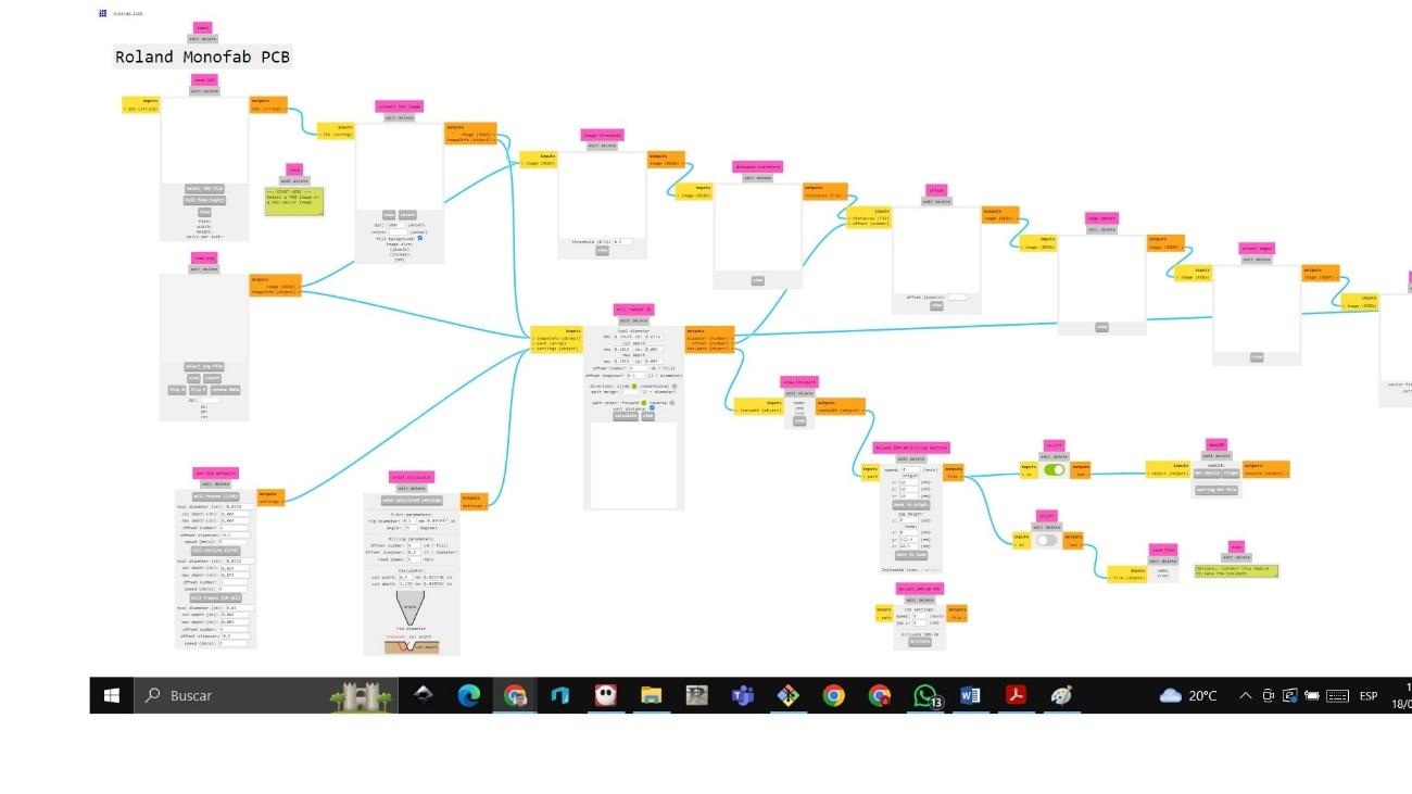
Configuration and use of Mods with the Monofab SRM-20
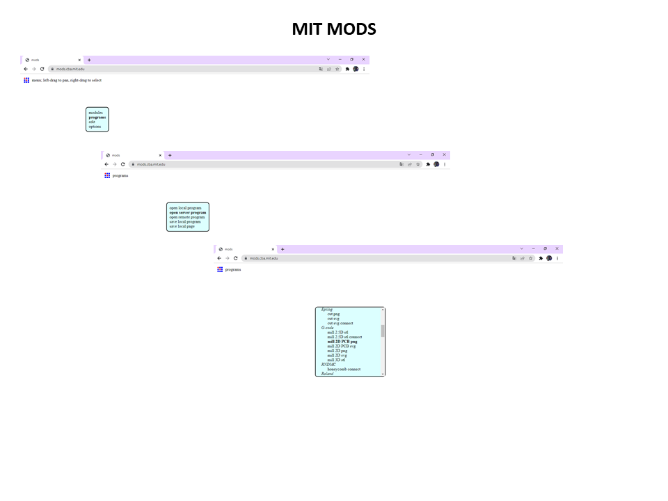
To control the machine we use the Mods software, which allows you to send the milling files directly to the SRM-20.
Pasos iniciales:
We open the direct access to Mods.
A terminal automatically opens where we verify:
Connection port (for example /dev/ttyUSB0 or similar depending on the device).
Flow control activated correctly.
At first we did not properly consider the port configuration and flow control, which caused the machine to not connect. This taught us that before we think there is a mechanical failure, we should check the digital settings.
Program settings in Mods
The default page is Mods Project.
Procedimiento:
Right click on the white screen.
Seleccionar: Programs.
Elegir: Open Server Program.
Ir a: Machines.
Buscar: Roland → SRM-20 → PCB png.
Luego:
In the Read PNG section, we load the file corresponding to the internal milling.
In tool type we select Traces (1/64) for milling internal tracks.
https://pub.fabcloud.io/tutorials/electronic_production/fabisp/
Milling parameters on the SRM-20
For the 2D milling raster we configure:
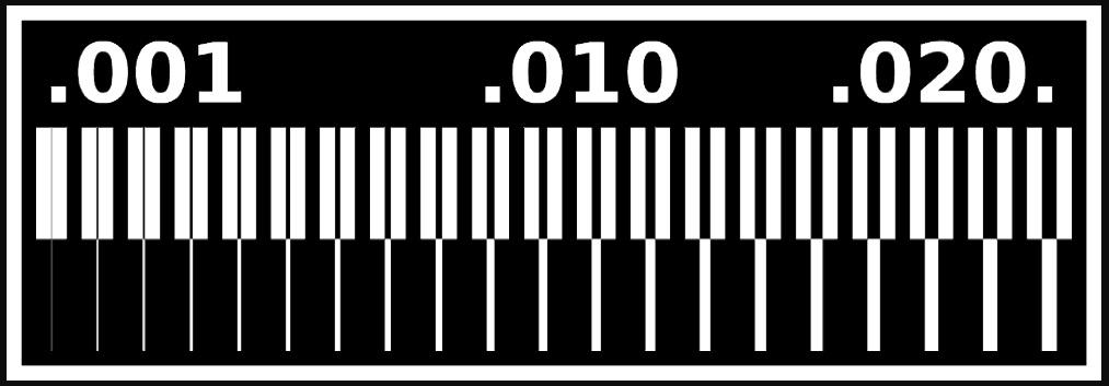
Profundidad máxima: 0.012 pulgadas
Number of passes automatically adjusted according to depth.
This parameter ensures that the machine removes copper accurately without damaging the base of the board.
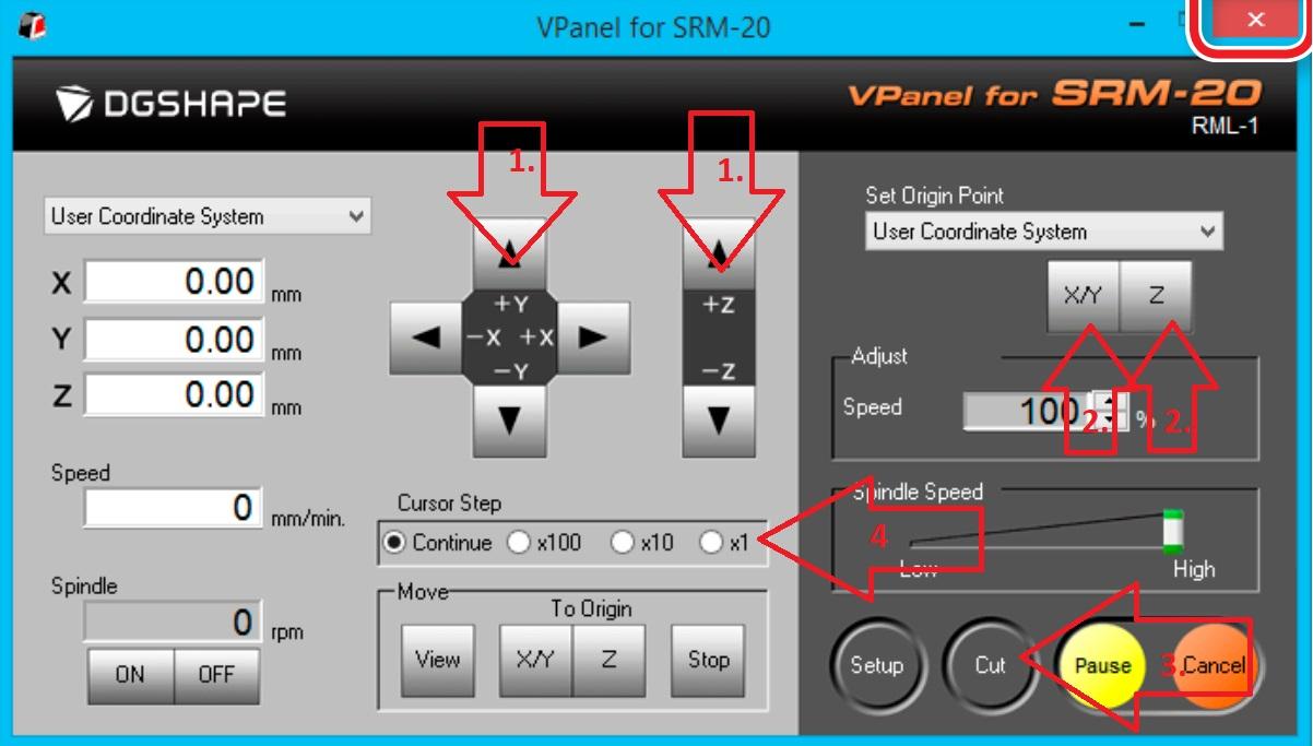
Axis calibration on the Monofab SRM-20
One of the most critical steps is manual calibration of the axes:
X and Y axis calibration:
From the machine control panel, we move the head to the point that we define as the origin, according to the location of the previously fixed board.
En mi caso:
X: aproximadamente 40 mm
Y: aproximadamente 20 mm
We then set that point as Set Origin X/Y.
Z axis calibration:
We slightly loosen the mill holding screw.
We manually lower the head until it is close to the surface of the board.
We gently drop the strawberry until it touches the plate.
We tighten the screw again to fix it.
Finalmente, configuramos Set Origin Z.
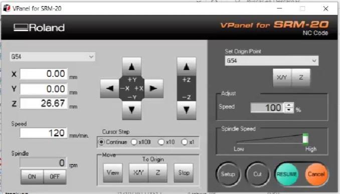
The bur should barely touch the surface. If you press too hard, you may break or mark the material before you start milling.
Start of milling
Once the parameters are configured and the origins are defined:
Presionamos Send File o Calculate → Send en Mods.
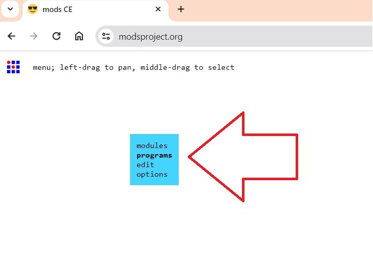
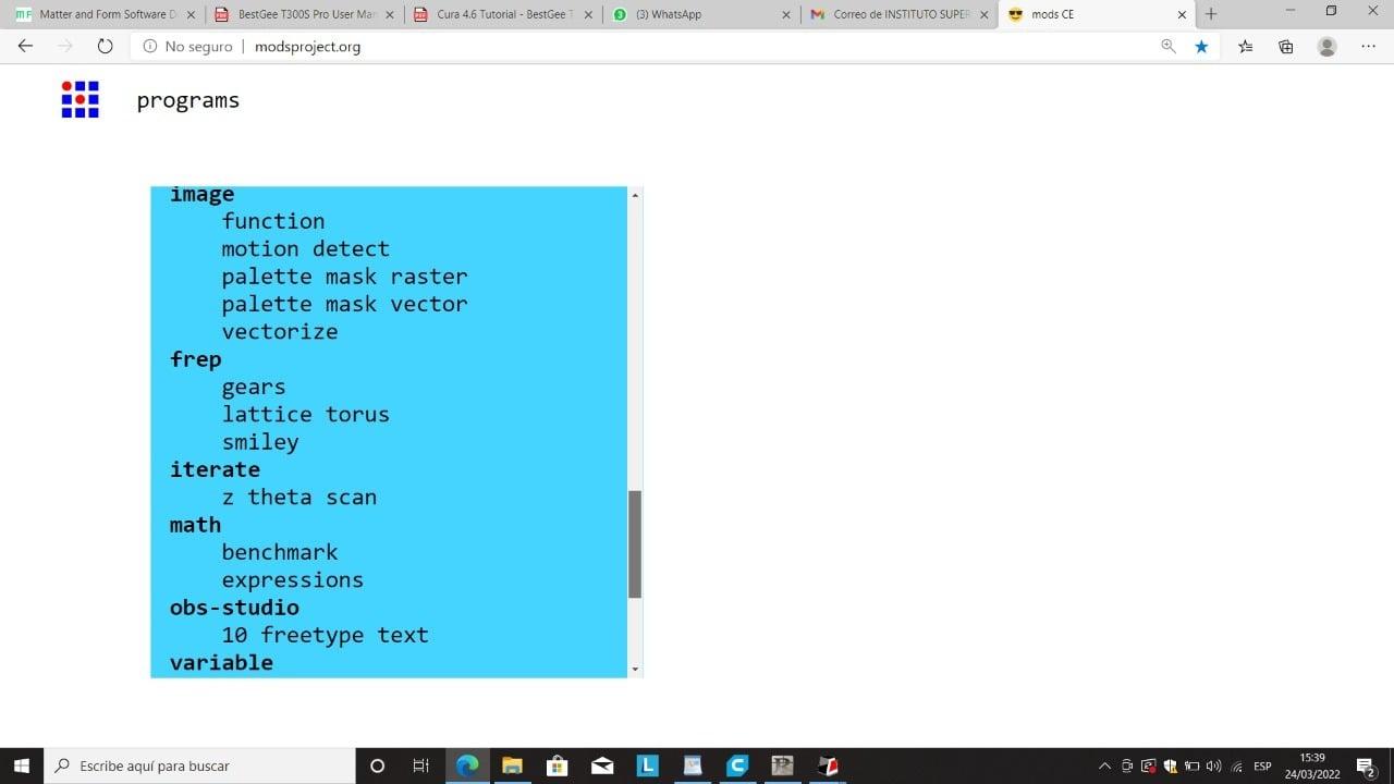
https://modsproject.org/
The machine starts the milling process automatically.
During work it is important to supervise the process without intervening, verifying that there are no vibrations or detachment of the material.
Edge milling
After finishing internal milling:
We change the tool for a 1/32 milling cutter for contour cutting.
We repeat the Z axis recalibration process.
We maintain the same origin in X and Y.
In Mods we select the file corresponding to the outline.
🏁 Completion of the process
At the end of milling:
We remove the mill first.
Then we use the spatula to carefully peel off the plate.
⚠️ You should never use leverage with the installed milling cutter, as it could bend or break.
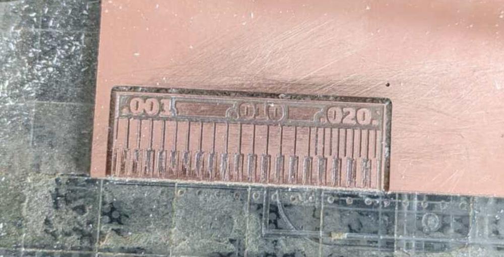
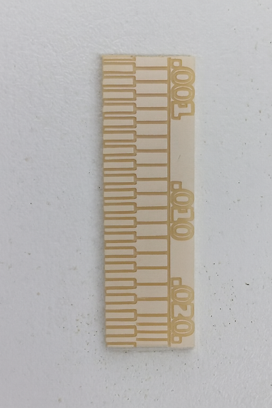
✨ Resultados obtenidos
The milling exercise with the Monofab SRM-20 showed well-defined tracks, clean cuts and precision in dimensions, demonstrating that correct calibration and digital configuration is decisive to achieve professional work.
In this collaborative work we organize ourselves strategically
🧠 Individual Assignment
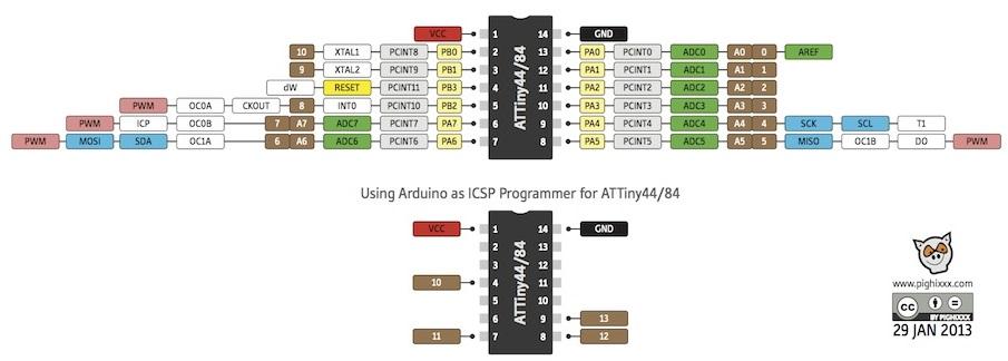
Microcontrolador ATTinny32:
This high-performance, low-power 8-bit AVR microcontroller is perfect for simple boards. The CPU must be able to access memories, perform calculations, control peripherals, and manage interrupts. Integrated ISP Flash memory allows program memory to be reprogrammed in the system, typically through an SPI serial interface.
The description of the ATTiny44/84 pin is as follows:
I first made this design based on Neil G. Fab's Tiny ISP-Board reference model.
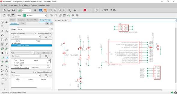
PCB Layout:
For PCB design with the Eagle IDE, see section 9.6.2. Previously, I had worked with Eagle version 6.5.0. However, I note that the current version is much more intuitive in several aspects. For ease of use, I add the eagle_fab.lbr library.
This is done in the Control Panel.
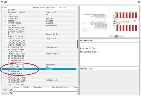
I then add the necessary electronic devices and components to the PCB.
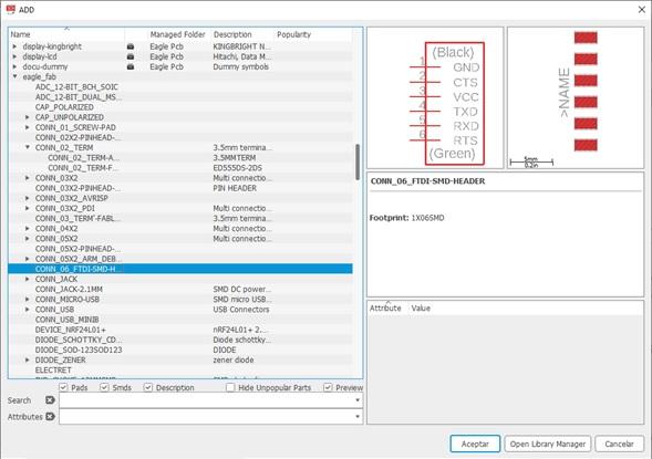
I add the FTDI output terminals
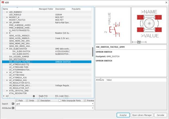
I add the switch
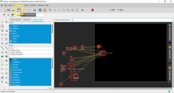
After adding all the components, I now have the PCB schematic with the components. All that remains is to organize and wire it. This is what the design looks like:
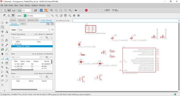
With the Network tool I make the lines used for the connections
Then I order and distribute the components.
Adding the connection points
Before finishing the schematic it should look like this:
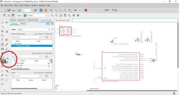
Then give the label or name to the components with the Name tool.
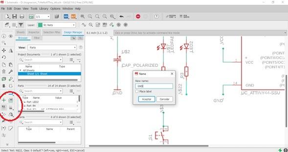
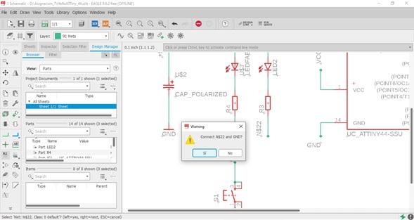
He asks me to connect, I say YES
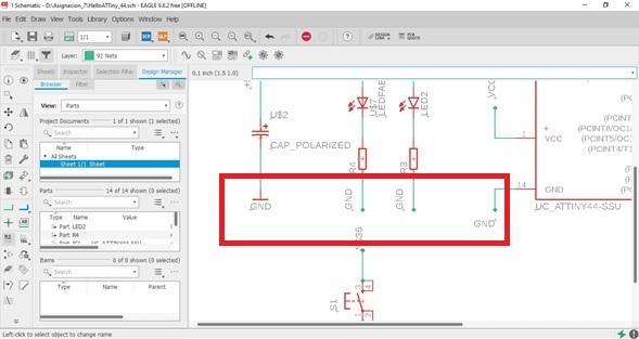
I have all the GND connections labeled.
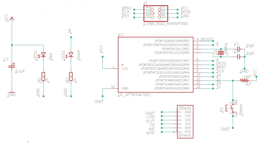
The final schematic looks like this:
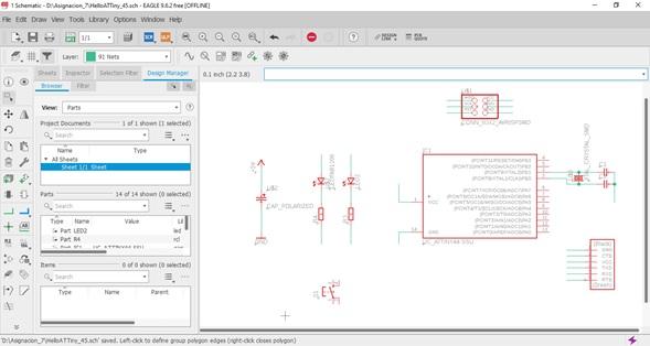
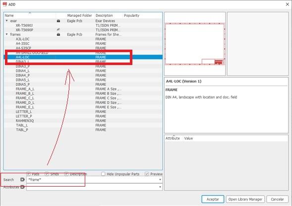
To finish I place a frame or legend box.
This is what the final schematic looks like:
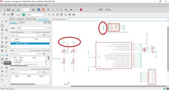
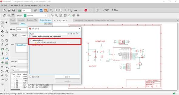
Before converting to PCB, I apply electrical rule checking (ERC) to the schematic. It gives me the following warnings:
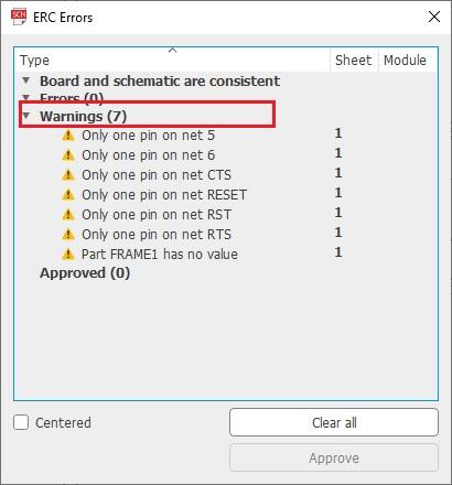
I start correcting the warnings one by one, before passing them to the PCB. Then it gives me a frame problem that doesn't matter when moving to the PCB. So far, I have the schematic ready.
Junta
Then, I click the BRD (Board) button to go to PCB (Printed Circuit Board) and start arranging the components.
Then I adapt the possible placement of the components and help me with their rotation. I model the placement of the components based on Neil's "Echo Hello" word board.
I correct the size (footprint) of the C3 capacitor, which was very large. I changed it to the SMD model.
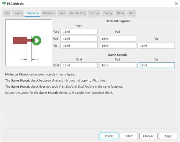
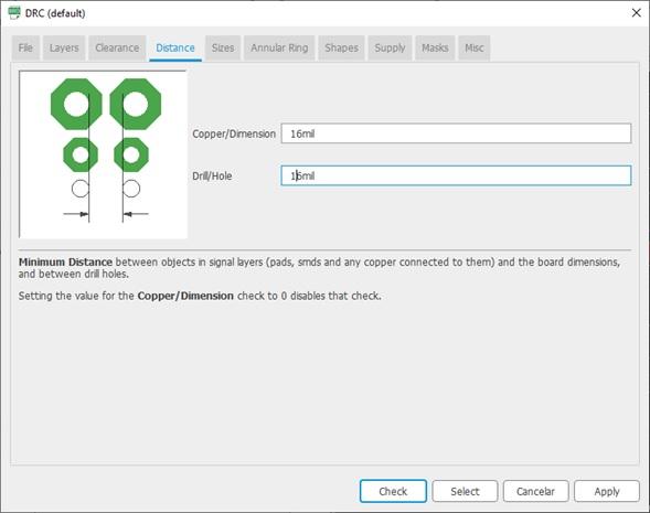
Add the design rule set (DRC) that helps us determine the minimum clearance between components. You can add it in the Tools > DRC menu, as shown below:
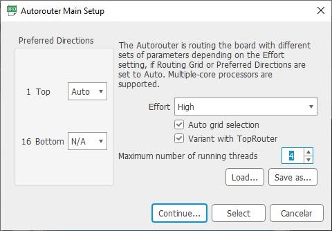
In auto routing, define only the top layer and create 4 threads
The distance will be 16 thousandths of an inch.
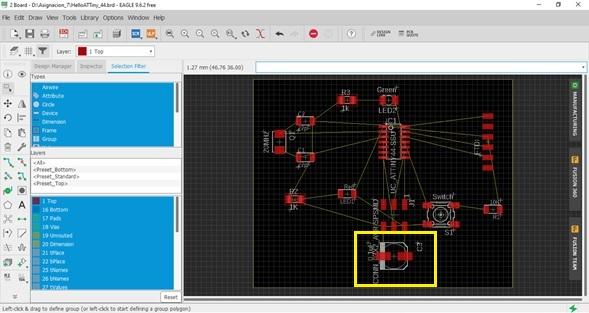
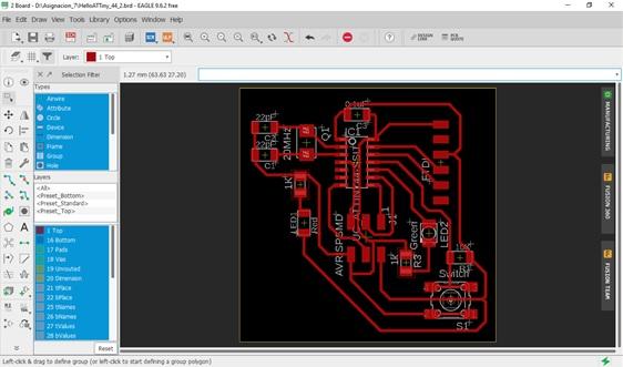
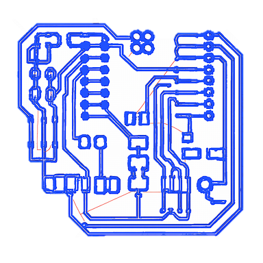
I finally got the PCB layout.
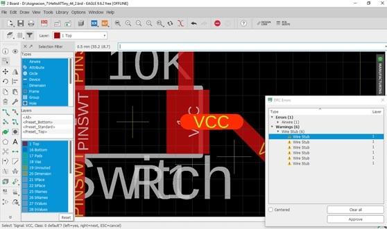
The DRC warns me of eight small pieces of loose wire. I am locating and eliminating them one by one.
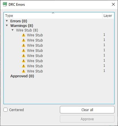
Remove a small Vcc wire that is duplicated.
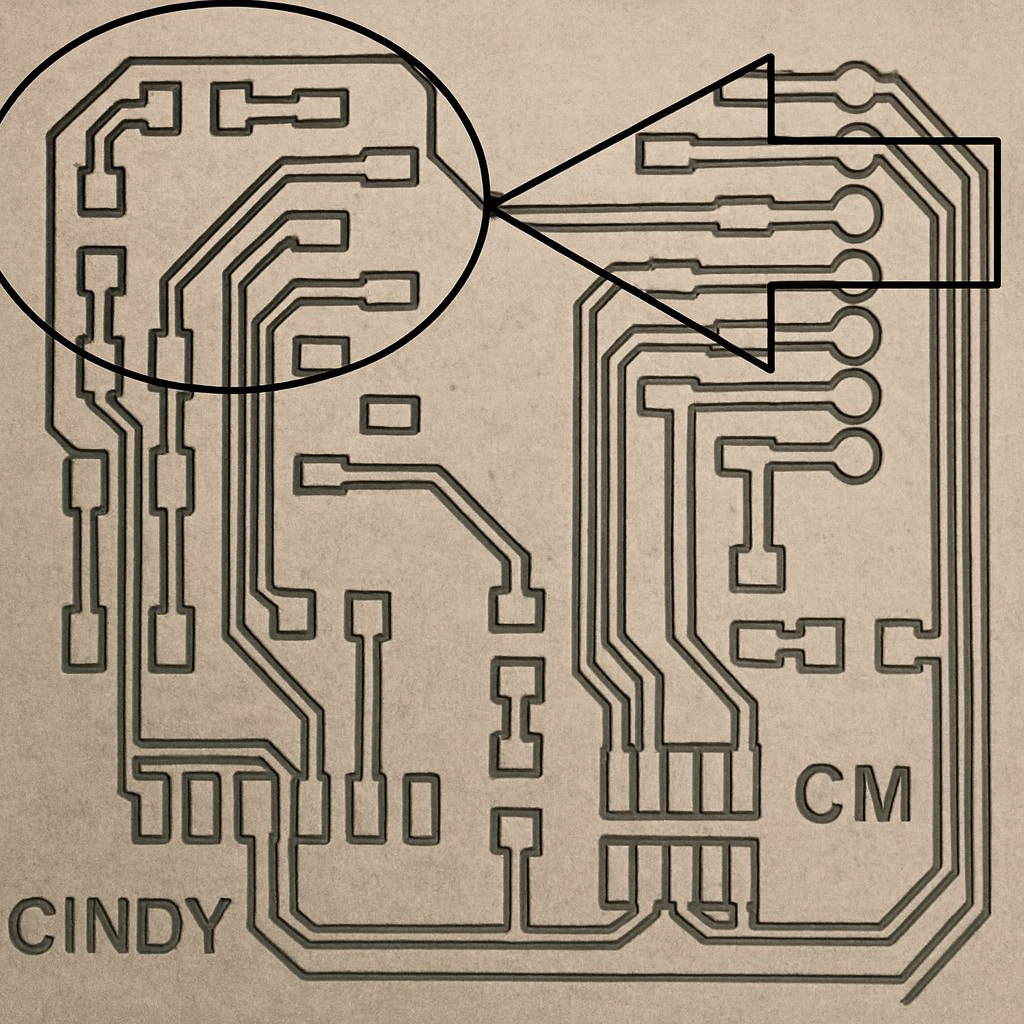
This is the route of the clues. I notice that I can reduce the size of the PCB by putting more components together.
El PCB terminado quedaría así
I add a couple of labels and adjust the outline frame.
I have the “Hello World” PCB ready
I filter the top layer, to do this I activate “Top” in the Eagle.
Now I only see the copper face
I then import the PCB as an image file in .png format
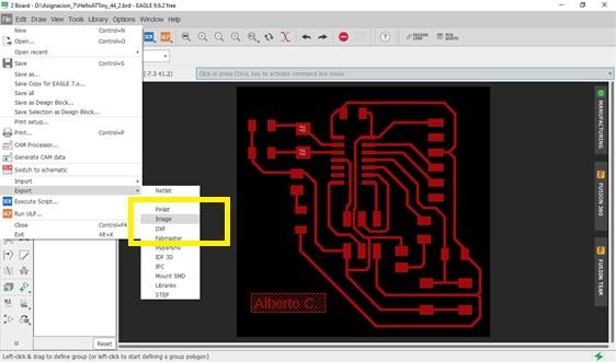
Export with 500 dpi resolution, full PCB size only and image in binary (monochrome)
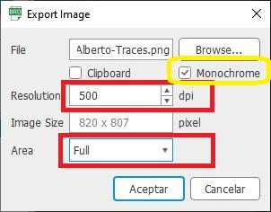
This way I get the PCB in actual size.
Card Milling and Assembly
In this practice I understood how electronic components work from the digital process to physical assembly. Although we did not initially have all the materials, we first worked on the computer to understand the complete milling flow before moving to the machine.
I learned that in digital manufacturing everything starts in the software. If I configure a parameter incorrectly, the error is transferred directly to the material.
Milling with software modifications
Paso 1
I downloaded the image in PNG format corresponding to the Card design, which I would use to do the milling.
Paso 2
I entered the modsproject.org page and with a right click I opened the program.
Paso 3
Seleccioné “Open Program”.
Paso 4
I chose the “Mill PCB 2D” option to configure the board milling.
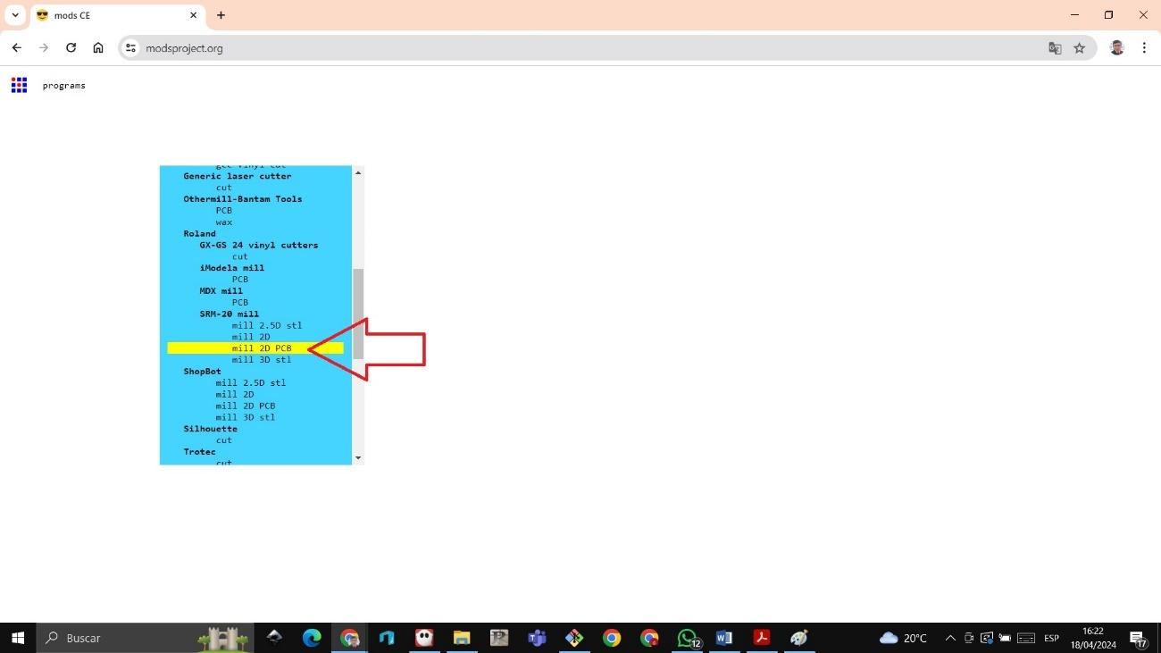
Paso 5
The interface appeared where I had to configure all the technical parameters.
Paso 6
Within the program I did the following:
I uploaded the PNG image of the design.
I selected the 1/64 fine milling cutter for milling the tracks.
I turned on the output to generate the cut file.
I set the X, Y and Z axes to define the start point.
I clicked on “Calculate” to generate the file with an .rml extension that I would later load into the SRM-20.
I observed on the screen the strokes that the milling cutter would make to manufacture the Card, which allowed me to digitally visualize the result before taking it to the machine.
Preparation on the SRM-20 Mini Milling Machine
Once the file was generated, I placed the board on the base of the SRM-20 and secured it with double-sided tape to prevent any movement during the process.
I then connected the software with the machine and proceeded to:
Calibrate the X, Y and Z axes.
Set the origin point.
Load the .rml file from the “Setup” button.
Check the travel speed of the cutter.
Here I understood that the calibration of the Z axis is one of the most critical points. If the bur is placed too low, it will break; If it is too high, it will not cut the copper correctly.
Milling adjustment
When I finished the first milling I carefully checked the plate and noticed that the upper right part had not been well defined. Therefore I decided to re-mill that section to improve the result.
This part taught me that in prototyping it does not always come out perfect the first time, and that it is necessary to correct until a good finish is obtained.
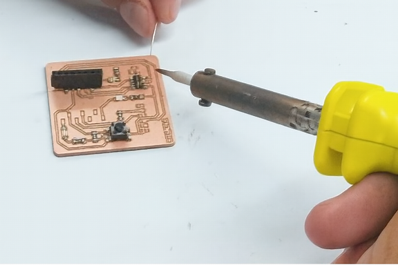
Component welding
With the board ready, I moved on to the board soldering process.
Utilicé:
Cautín
Estaño
soldering paste
It was my first time soldering electronic components, so it was complicated at first. I had a hard time controlling the amount of tin and keeping my pulse steady. However, with practice I managed to improve.
I soldered resistors, LEDs, sockets and switch. It had to be very precise, as the XIAO ESP32 3C microcontroller had to fit correctly into the sockets.
Although the solder was not aesthetically perfect, it managed to make contact and allow the circuit to function.
Programación y prueba final
The time has come to test the Card.
I opened the Arduino software, selected the XIAO ESP32 3C model and connected it.
I wrote the program that stated the following:
If the switch is pressed, the LED turns on and off 10 times with an interval of 1 second.
If not pressed, the LED remains off.
I loaded the program and verified the operation directly on the board.
When the LED responded correctly to the switch, I confirmed that the entire process—from milling to soldering and programming—had been successful.
Conclusiones
Using the SRM-20 Mini Milling Machine was a challenging and demanding process. Understanding the software, correctly calibrating the Z axis, and manipulating the cutter accurately was essential to prevent it from breaking, something that happened to me on a few attempts when I placed it too low.
Soldering also presented difficulties at the beginning, but I managed to complete the assembly functionally.
This experience not only allowed me to manufacture an electronic board, but also strengthened my precision, patience, and technical judgment in the use of digital manufacturing tools.
The Card represents my hands-on learning in milling, assembly and programming of electronic systems.
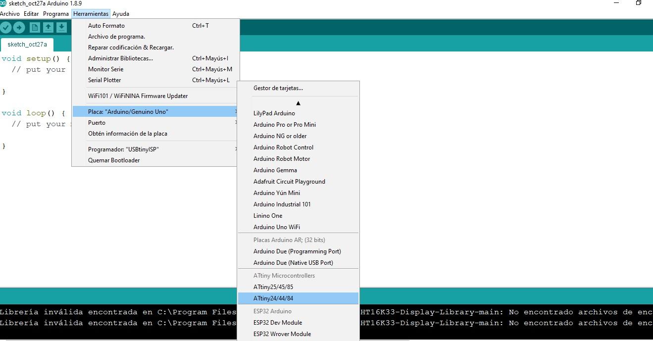
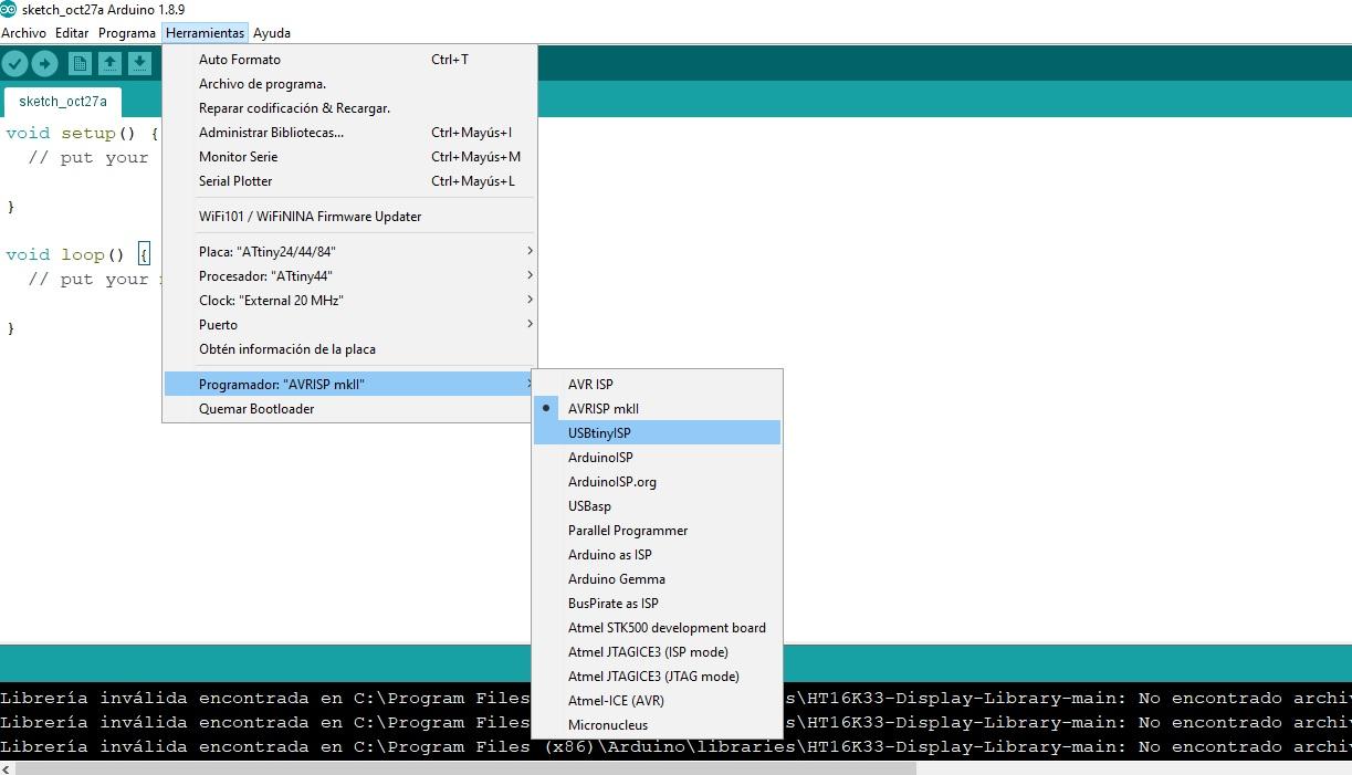
In the Arduino IDE, I go to tools and select the ATtiny44 board and processor.
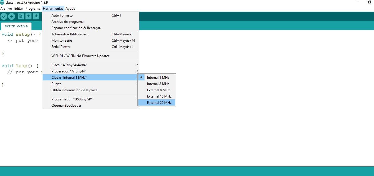
The crystal I used for the PCB is 20 MHz, so I select an external 20 MHz clock.
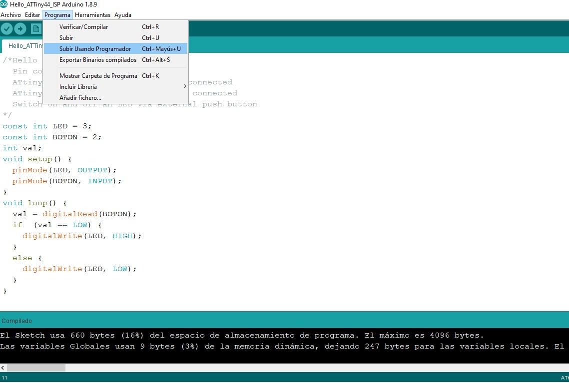
Next, I chose “Hello ATTiny44”, for this I chose the FabTinyISP Scheduler in USBtinyISP mode.
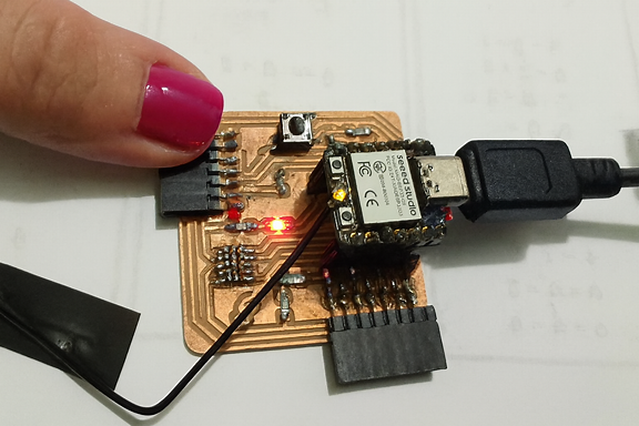
Now I use a program “Hello ATTiny44” that, through a button connected to PA2 (pin11), lights an LED connected to PA3 (pin10), based on the designed PCB.
/*Hello ATTiny44A
Pin configuration:
ATtiny44 PA3 (pin 10)--> Green LED connected
ATtiny44 PA2 (pin 11)--> Pushbutton connected
Switch on and off an LED via external push button
*/
const int LED = 3;
const int BOTON = 2;
int val;
void setup() {
pinMode(LED, OUTPUT);
pinMode(BOTON, INPUT);
}
void loop() {
val = digitalRead(BOTON);
if (val == LOW) {
digitalWrite(LED, HIGH);
}
else {
digitalWrite(LED, LOW);
}
}
The next step is to write the program “Hello Attiny44” on the microcontroller. If everything goes well, it will be a success.
https://photos.google.com/share/AF1QipOwTZzTzNoa_QpuG_plUoZsT5GqI_YGMvr_y3HGaNrgjTzr27PEaf0JI2DrM3CYhw?key=bjFmNTlVLWdzZkVTQ3VjNVgyRnMyXzh6TWk2V1RR