Electronics Design
Semana 06:
Electronics Design – Fab Academy
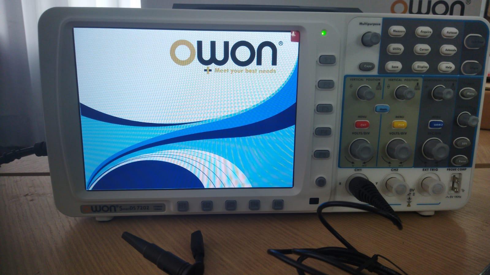
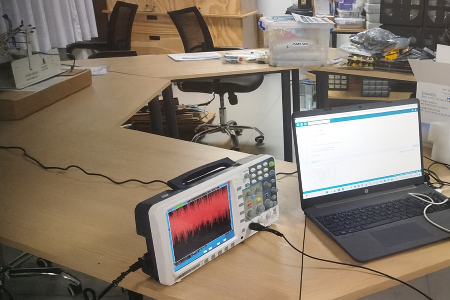
In this group work from Cerro de Pasco we met with my colleague Renso and from the city of Huánuco with our colleague Ronal via Google Meet, to be able to interact and compare the operation of the oscilloscope, which in our case is the WON SmartDS 7202.
Owon SDS7202 series SmartDS deep memory storage digital oscilloscope with VGA interface, 2 channels, 60 MHz, 500 MS/s sampling rate. Characteristics:
Development of Group Practice
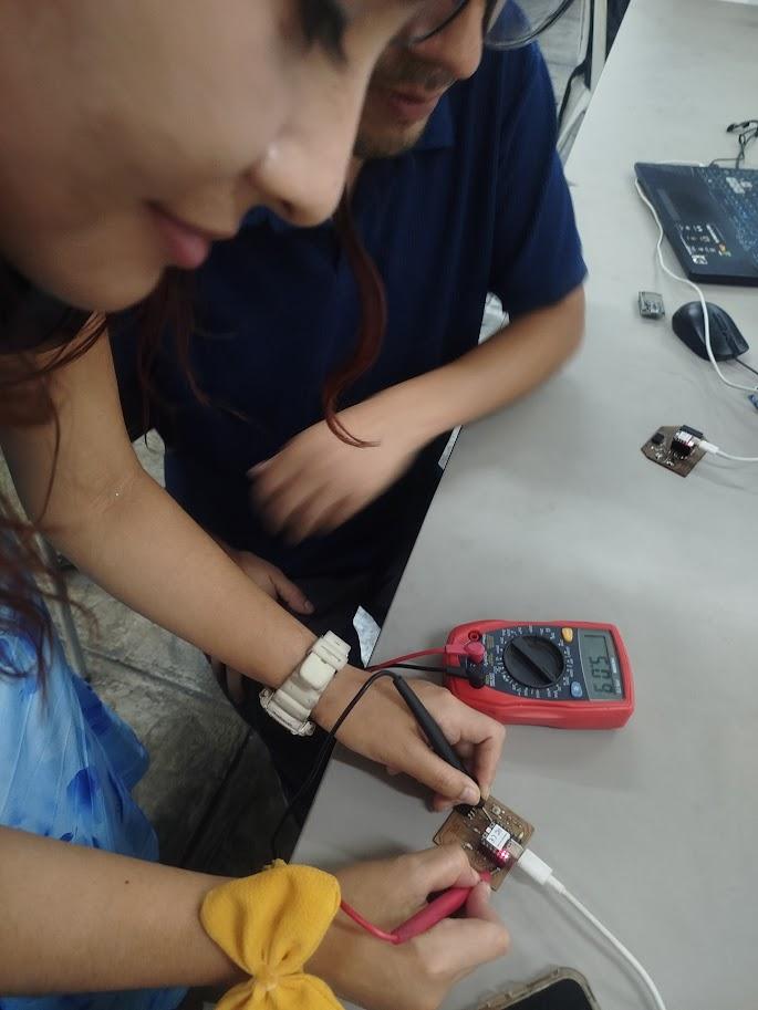
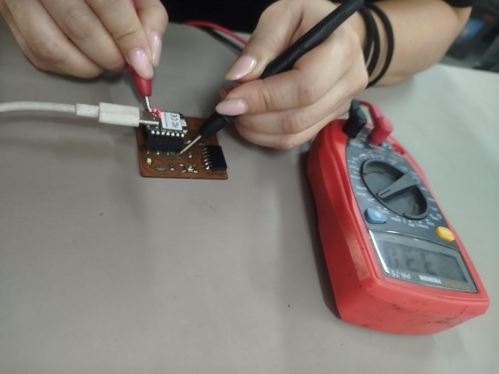
PROBANDO MULTIMETRO VS OSCILOSCOPIO
We developed a fully synchronized technical session, comparing results in real time and analyzing the behavior of the signals using the OWON SmartDS SDS7202 oscilloscope.
Osciloscopio Digital OWON SmartDS SDS7202
The equipment used was a deep memory storage digital oscilloscope, model OWON SDS7202, a robust instrument designed for electronic design, diagnostics, maintenance and academic training applications.
Among its main technical characteristics are:
Dos canales independientes.
60 MHz bandwidth.
Maximum real-time sampling rate of 250 MS/s per channel.
Recording length of 10 Mpts per channel, allowing waveforms to be captured with a high level of detail.
Funciones matemáticas integradas, incluyendo FFT.
20 automatic measurements for advanced analysis.
Pantalla TFT LCD de 8” a color.
VGA port for external display.
Advanced trigger system for stabilization of complex signals.
This equipment allowed us to observe not only the amplitude of the signal, but also its stability, noise and dynamic behavior.
Multímetro Digital S-75
We also use the S-75 digital multimeter, which has the following specifications:
Voltaje máximo: 500 V DC / 500 V AC.
Protection fuse: 200 mA / 250 V.
Power: 9V battery.
1999 count LCD display with illumination.
Measurement method: dual slope A/D integration.
Rango operativo: 0 °C a 40 °C.
Battery indicator on screen.
Compact dimensions and approximate weight of 280 g.
This instrument was key to quantitatively validate the voltage values obtained in the tests.
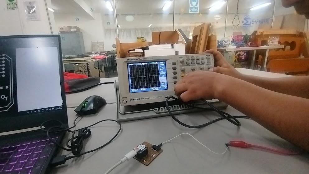
Tests with the Oscilloscope
Teamwork using the oscilloscope
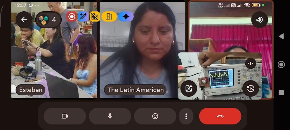
During the session we coordinated each step, making sure that we were all measuring under the same conditions.
Preparing the equipment for ignition
We verify connections, condition of the tips and initial calibration before beginning any measurement.
Power on the equipment
By pressing the power button we observe the main interface and configure channel 1 to begin measurements.
Connecting the test leads
Conectamos cuidadosamente:
Ground tip (GND).
Signal tip to the output pin of the potentiometer.
This step was crucial to avoid noise or erroneous readings.
Signal amplitude adjustment
We configure the vertical scale (Volt/div) and horizontal scale (Time/div) to correctly display the generated signal.
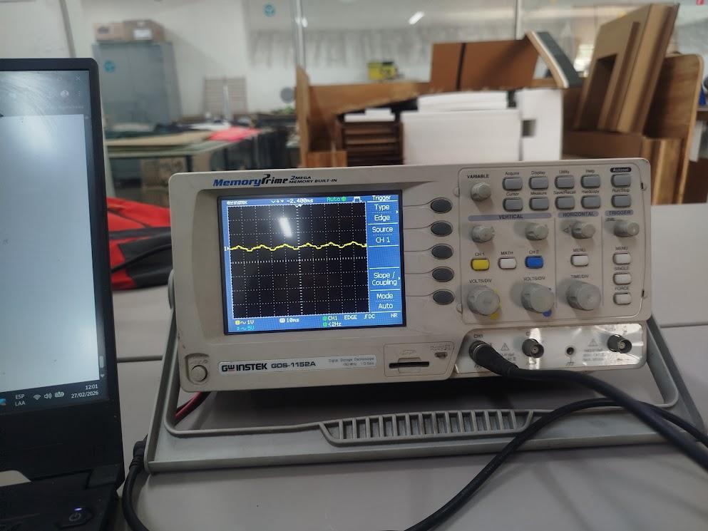
Display with potentiometer at low value
When the potentiometer was at its minimum value, the signal showed a reduced amplitude, evidencing a low level of voltage at the output.
Potenciómetro al 50%
By increasing the value to the midpoint, we observed a proportional increase in the signal amplitude, which confirmed the expected linear behavior of the component.
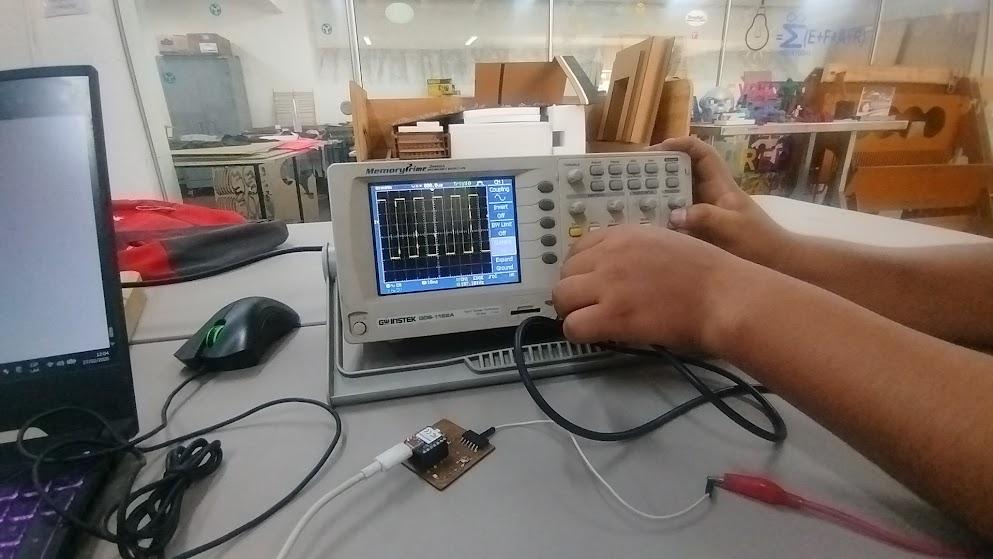
Potenciómetro al valor máximo
With the potentiometer at maximum, the signal reached its highest amplitude within the power range, showing stability and minimal distortion.
Signal expansion
By adjusting the horizontal scale we were able to analyze the waveform in greater detail, observing small variations and possible interferences.
Setting for cleaner signal (low value)
We reduce the vertical scale and adjust the trigger to stabilize the signal, obtaining a more precise visualization.
Setting for cleaner signal (high value)
With the potentiometer raised, we adjust the parameters again to avoid visual saturation and keep the signal centered on the screen.
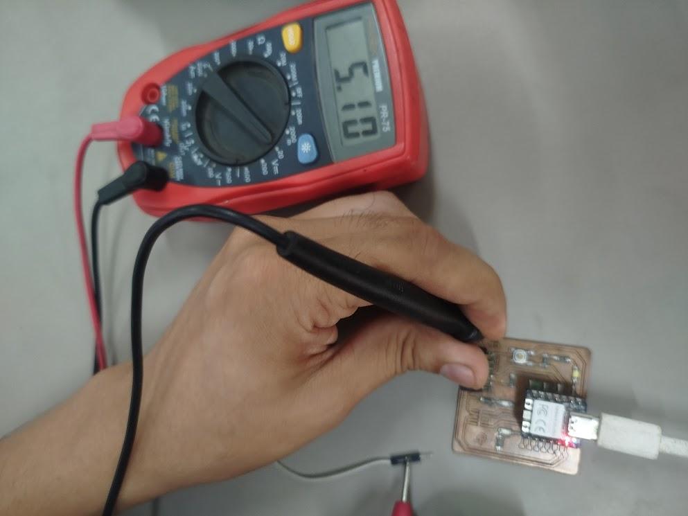
Tests with the Multimeter
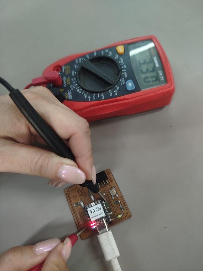
Measuring the 5V input
We confirmed that the supply voltage to the potentiometer was approximately 5V DC, validating that the source was correctly supplying power.
Measurement at 10% of the potentiometer
When the potentiometer was at 10% of its travel, the multimeter showed a proportionally low output, confirming the expected resistive behavior.
Measurement at 80% of the potentiometer
By raising the value to 80%, the measurement indicated a significant increase in the output voltage, demonstrating the continuous and controlled variation of the component.
Reflexión Final
This work did not only consist of measuring signals; It was an experience of collaborative technical analysis. I understood the difference between visualizing a signal and understanding it.
The oscilloscope allowed me to observe the dynamic behavior of the signal in real time, while the multimeter gave me the exact value in numerical terms.
Working as a team from different cities demonstrated that engineering has no physical borders when there is coordination and technical criteria.
Here we not only use instruments; We learned to interpret what really happens inside the circuit.
Referencias
GW Instek GDS-1152A Oscilloscope Documentation https://www.gwinstek.com
Basic Oscilloscope Operation Guide https://learn.sparkfun.com/tutorials/how-to-use-an-oscilloscope
Seeed Studio XIAO RP2040 Documentation https://wiki.seeedstudio.com/XIAO-RP2040/
🔷 INDIVIDUAL ASSIGNMENT
🔎
Tarea individual

1. Choice of circuit design program
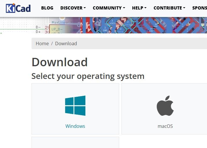
To start in the world of electronic circuit design, KiCad was selected, a free software widely used for the design of electronic schematics and printed circuit boards (PCB). This program allows you to develop complete projects, from the electrical diagram to the final design of the electronic card.
2. Installation platform selection
In this case, it was chosen to install the KiCad program on the Windows operating system, due to its compatibility, ease of installation and extensive support for electronic design tools.
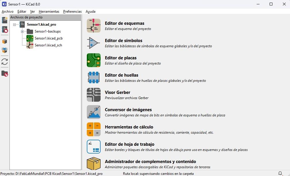
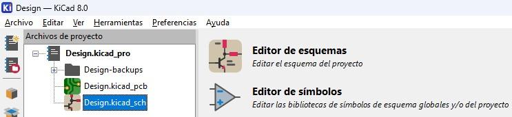
3. Observation of the program environment
Once the program finishes loading, you can see the main KiCad environment, where the different tools available for creating electronic projects are displayed, such as the schematic editor, the PCB editor and library configurations.
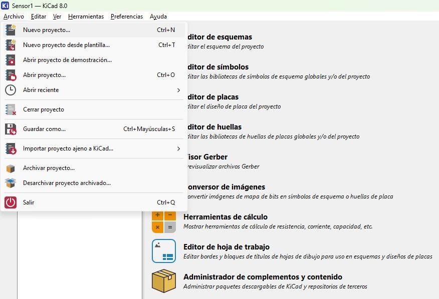
4. Creation of a new project
To start the work, select the New Project option, which allows you to create a workspace where all the files related to the design of the electronic circuit will be stored.
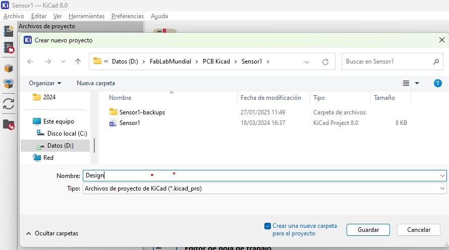
5. Storage drive selection
Subsequently, choose the system drive or folder where the new project will be created. This location will allow you to save all the files necessary for the development of the electronic circuit.
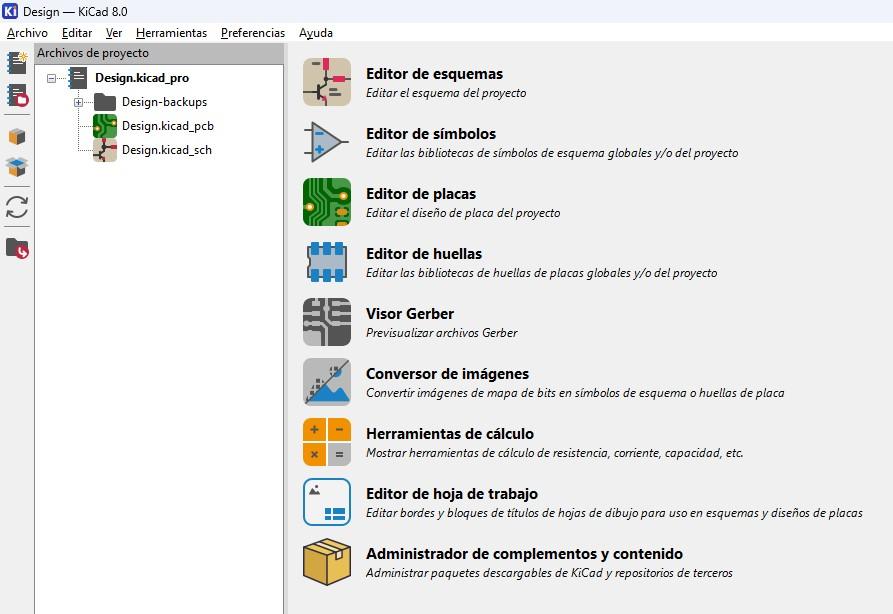
6. Archivos generados automáticamente
When creating the project, the system automatically generates two main files:
PCB: file intended for the design of the electronic card or printed circuit board.
SCH: file where the electrical diagram of the circuit is developed.
These files will be used during the circuit design and manufacturing process.
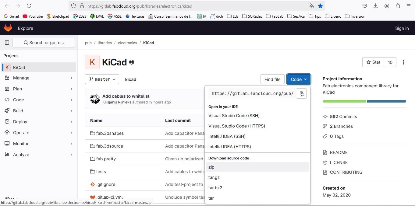
7. Download libraries from GitHub
To work with the necessary components, the electronic components library used in FabAcademy is downloaded from GitHub, which is in ZIP format. This library contains the symbols and traces necessary for the design of the circuits.
8. Access to the symbol editor
Once the library has been downloaded, the Symbol Editor is accessed from the KiCad environment to be able to install and manage the new electronic component libraries.
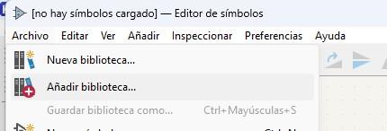
Add symbol library
Within the editor, the option File → Add Library is selected, which will allow the new downloaded library to be incorporated into the system.
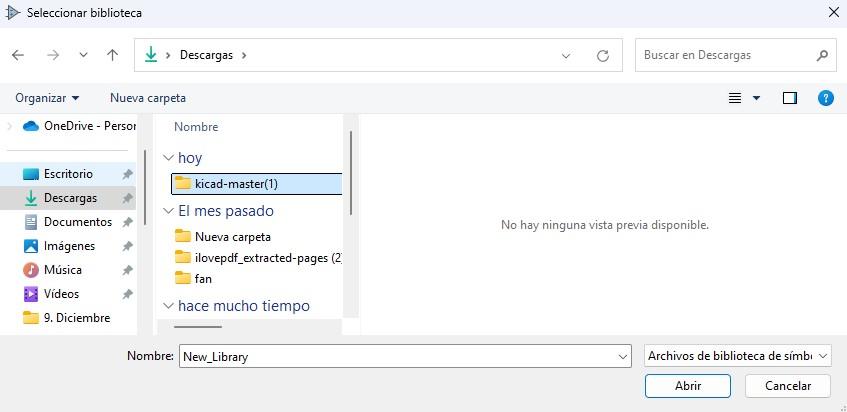
10. Selecting the unzipped folder
Subsequently, the folder where the downloaded library was unzipped is searched, selecting the corresponding file to integrate it into the program.
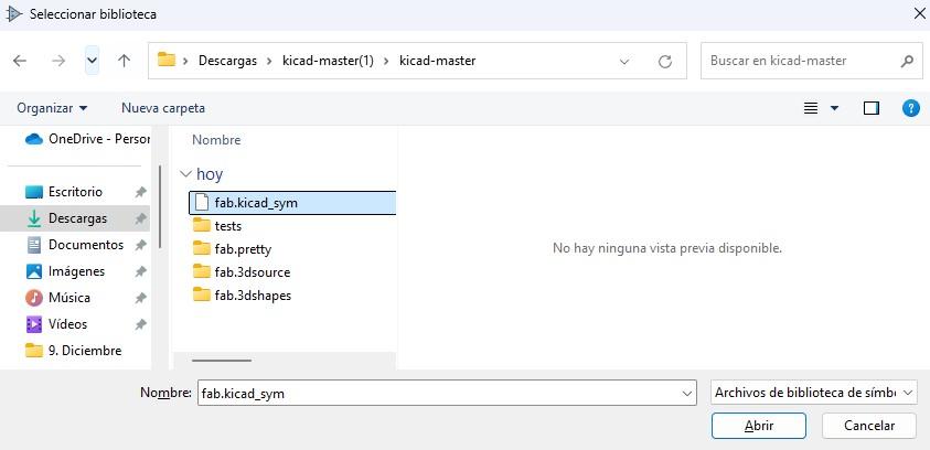
11. Component file selection
Within the folder, choose the file that contains the symbols of the electronic components, which will be added to the KiCad library for later use in the design of the scheme.
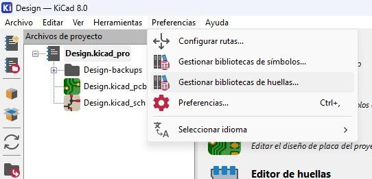
12. Footprint Library Management
Then you access the option Preferences → Manage fingerprint libraries, where the physical fingerprints of the components that will be used in the design of the electronic board will be configured.
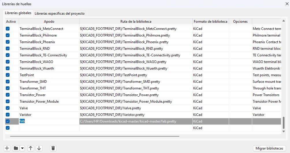
13. Add footprint library
In this section, select the + symbol to add a new library, assigning a nickname (nickname) and selecting the folder where the fab.pretty library is located.
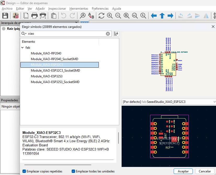
14. Insertion of the microcontroller into the schematic
Finally, within the schematic editor, select the Add component option and search for XIAO, which will be the main microcontroller of the project. Once selected, you can see that the component is already available in the library and ready to be used in the circuit design.
We open the Arduino UNO file
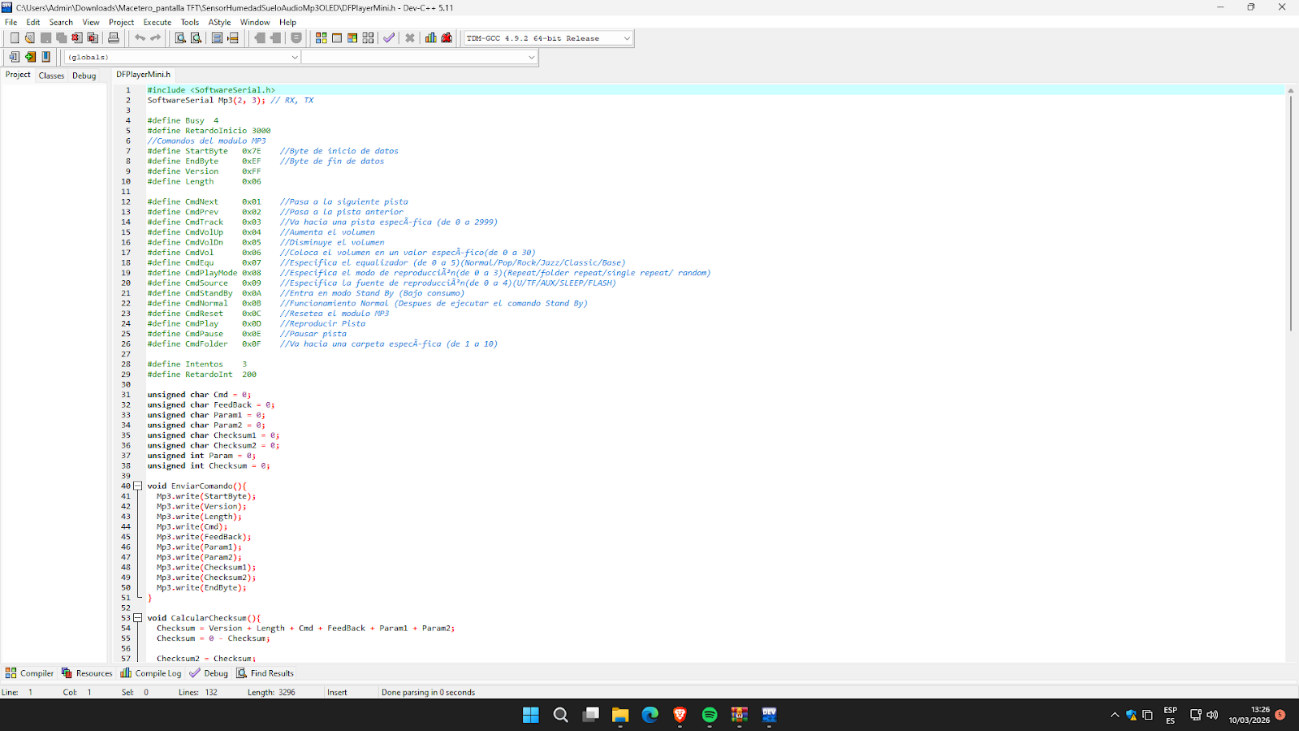
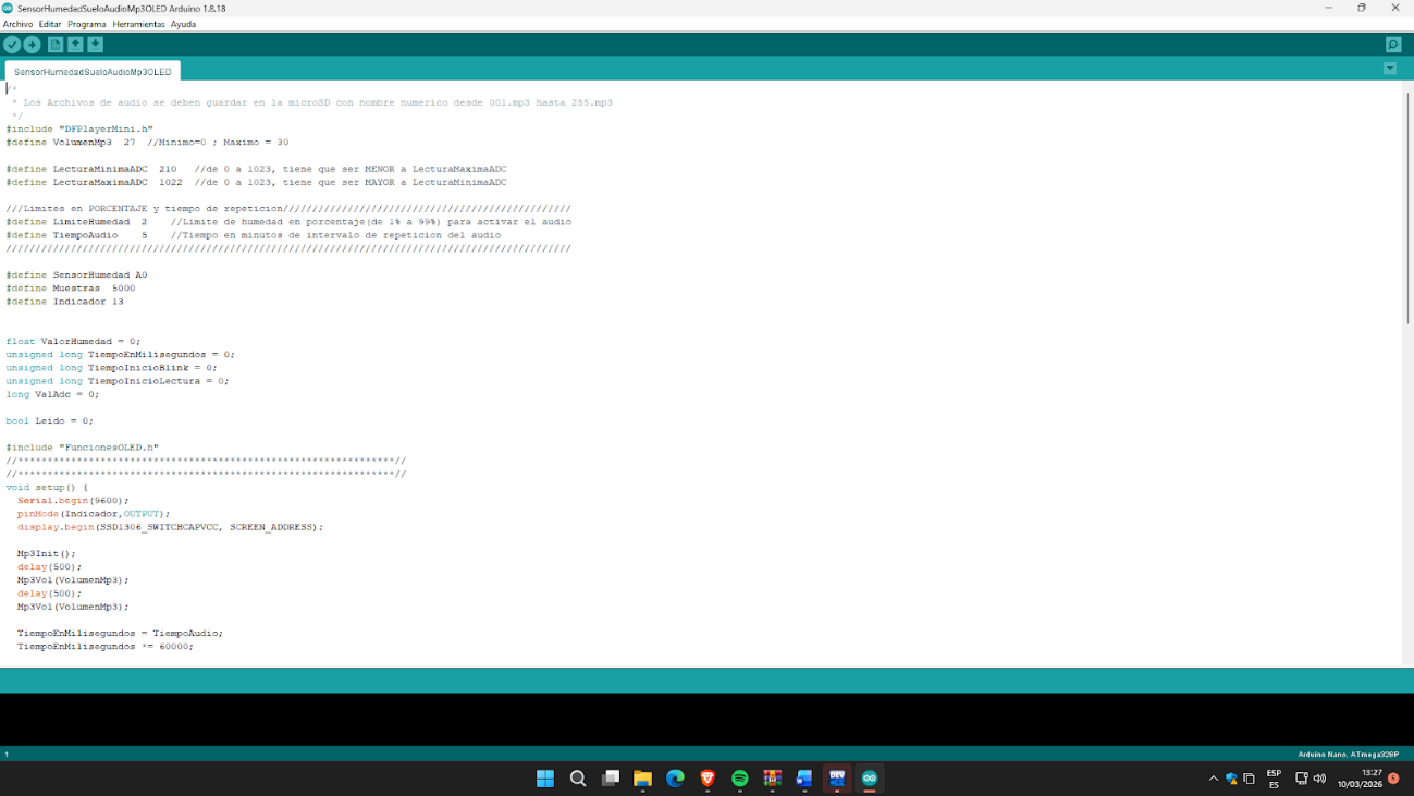
1. Writing the code in the programming environment
In this stage, the code is written in the programming environment, which will allow controlling the operation of the electronic circuit. This code defines the behavior of the microcontroller, indicating how it should react to the interaction with the button and how to control the lighting of the LED.
Hardware connection to the programmer
Subsequently, the connection of the electronic board, which contains the LED and the button, to the programmer is made. This programmer acts as an intermediary between the microcontroller and the computer, allowing the developed code to be transferred to the board.
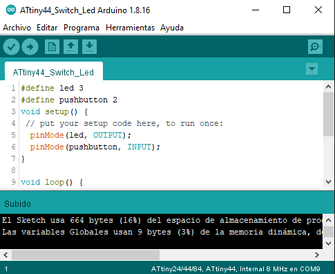
3. Loading the program on the board
Once the connections are established, the “Upload using the scheduler” option is selected within the programming environment. This action allows the previously written code to be compiled and transferred to the microcontroller, starting the board programming process.
4. Confirmation of program loading
After completing the upload process, the system displays the “Uploaded” message at the bottom of the screen. This message confirms that the code was successfully transferred to the microcontroller and that the circuit is ready to execute the programmed instructions.
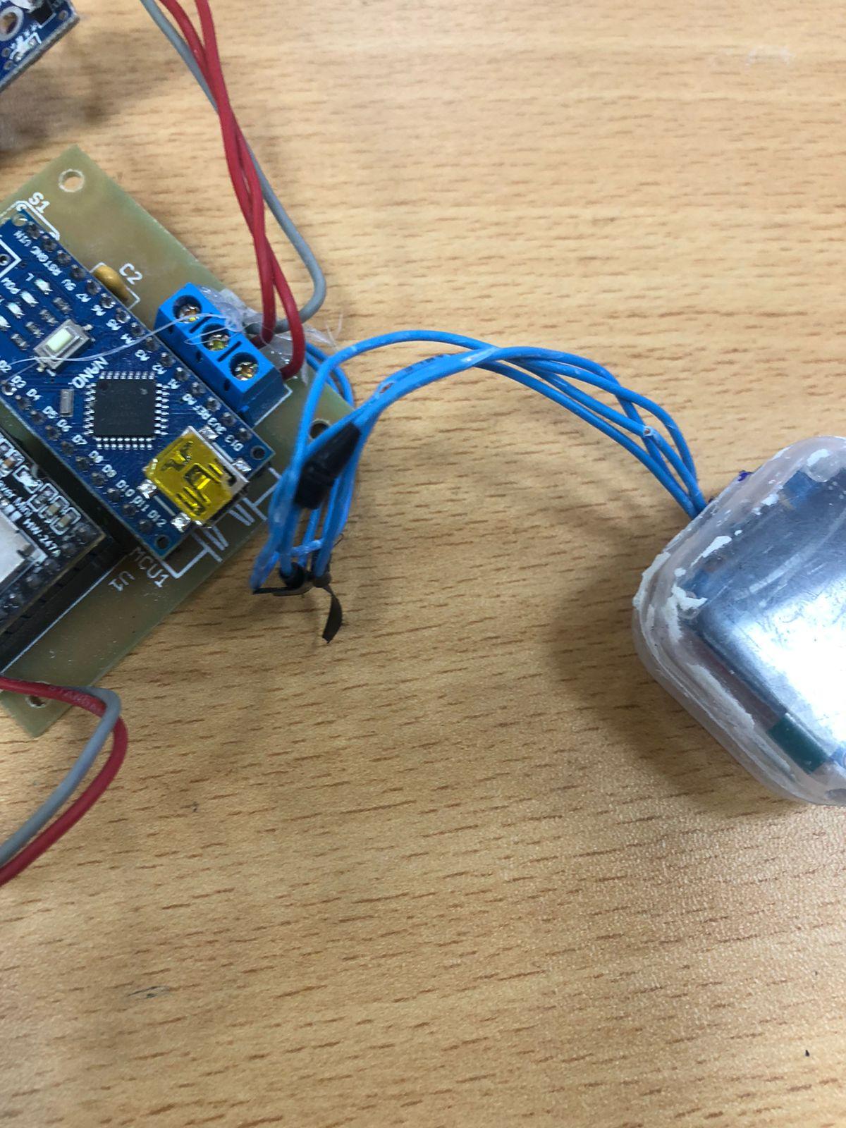
5. Implementation of the circuit on the breadboard
Finally, a breadboard is used to power the electronic board and perform circuit functional tests. In this stage, the LED and the button are connected, allowing us to verify that the system responds correctly to the user's actions as defined in the code.
Archivos
Macetero A